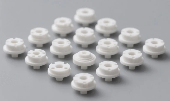
5-Axis Milled Ceramic Insulators for Semiconductor Equipment & Cleanrooms

In the high-stakes world of semiconductor manufacturing and cleanroom environments, every component must deliver flawless performance. At PFT, we specialize in crafting 5-axis milled ceramic insulators that redefine precision and reliability. With over 20+ years of expertise, our solutions are engineered to meet the exacting demands of semiconductor equipment, ensuring thermal stability, electrical insulation, and contamination-free operation in ultra-sensitive settings.
Why Choose Our 5-Axis Milled Ceramic Insulators?
1. Advanced Manufacturing Capabilities
Our facility is equipped with state-of-the-art 5-axis CNC milling machines, enabling micron-level accuracy in shaping advanced ceramics like alumina (Al₂O₃), silicon carbide (SiC), and aluminum nitride (AlN). Unlike conventional methods, 5-axis machining allows for complex geometries—critical for components like wafer lift pins, deposition chamber parts, and plasma-resistant insulators .
Key Features:
• Precision: ±0.005mm tolerance for seamless integration into ASML lithography tools or Lam Research etch systems.
• Material Versatility: Optimized for 99.8% alumina, high-purity SiC, and other advanced ceramics.
• Surface Finish: Ra <0.2μm to minimize particulate generation in ISO Class 1 cleanrooms.
2. Proprietary Process Engineering
Our engineers have developed closed-loop process controls that adapt to ceramic’s brittleness during machining. By combining dry milling techniques with real-time vibration damping, we achieve crack-free surfaces and extended component lifespans—even under extreme thermal cycling (up to 1,600°C) .
Innovation Spotlight:
• Stress-Relief Protocols: Minimize micro-fractures in AlN insulators for CVD applications.
• Post-Machining Treatments: HIP (Hot Isostatic Pressing) enhances density and corrosion resistance.
3. Rigorous Quality Assurance
Every insulator undergoes 12-stage inspection, including:
• CMM (Coordinate Measuring Machine) validation of critical dimensions.
• Helium leak testing for vacuum compatibility.
• EDS (Energy-Dispersive X-ray Spectroscopy) to verify material purity.
Our ISO 9001/14001-certified system ensures traceability from raw material procurement (sourced from Tier 1 suppliers like CoorsTek) to final packaging .
Applications: Where Precision Meets Performance
Our insulators are trusted in:
• Etch & Deposition Tools: SiC-coated components for plasma resistance in Applied Materials™ modules.
• Ion Implanters: Alumina lift pins with anti-static coatings to prevent wafer slippage.
• Metrology Systems: Low-thermal-expansion insulators for EUV lithography stages.
Case Study: A leading semiconductor OEM reduced tool downtime by 40% after switching to our custom-designed SiC showerheads, which outperformed competitors’ parts in 300mm wafer processing .
Beyond Manufacturing: A Partnership Approach
• Rapid Prototyping: Submit your CAD files and receive functional prototypes in 7 days.
• On-Site Cleanroom Packaging: Optional Class 10 cleanroom assembly for direct tool integration.
• Lifetime Technical Support: Our engineers provide wear analysis and re-machining services to extend component lifecycles.


Q:What’s your business scope?
A: OEM Service. Our business scope are CNC lathe processed, turning,stamping,etc.
Q.How to contact us ?
A:You can send inquiry of our products,it will be replied within 6 hours;And you can contact dirrectly with us through TM or WhatsApp, Skype as you like.
Q.What information should I give to you for inquiry?
A:If you have drawings or samples,pls feel free to send us,and tell us your special requirements such as material, tolerance, surface treatments and the amount you need,ect .
Q.What about the delivery day?
A: The delivery date is about 10-15 days after receipt of payment.
Q.What about the payment terms?
A: Generally EXW OR FOB Shenzhen 100% T/T in advance,and we can also consult accroding to your requirement.


